

The COVID-19 continues to spread globally. At the time of writing this article (July 20, 2020), 14.3 million people worldwide have been infected, and the death toll exceeds 600,000.
At present, the trend of the spread of COVID-19 is increasing, so countries around the world continue to "lock the door"! As a result, demand in the manufacturing industry has declined, the supply chain of parts and materials has been interrupted, and companies have generated huge deficits. More and more companies are unable to make their performance expectations for the next fiscal year.
However, the semiconductor industry has not been affected by the new crown pneumonia. For example, Taiwan’s TSMC, which is at the top of the miniature processing technology, has mass-produced the world’s most advanced exposure equipment EUV with 5nm node ("node" is omitted below) technology. In addition, TSMC It also plans to start 3nm risk production in October and mass production in 2021. In addition, TSMC has officially started research and development of 2nm, and plans to start 2nm risk production in the second half of 2021.
At the same time, South Korea's Samsung Electronics has been following TSMC. That is to say, despite the global crisis of the new crown pneumonia, the semiconductor miniaturization technology has not stagnated, but has accelerated its development.
So, what about the shipment value of semiconductors and semiconductor production equipment? As shown below.
Sales Volume of Semiconductors and Semiconductor Production Equipment
The transition in the sales volume of semiconductors and semiconductor production equipment from 1991 to 2019, and 2020 is the forecast value.
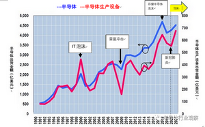
According to WSTS (World Semiconductor Trade Statistic, World Semiconductor Trade Statistics Association) forecasts, compared with the downturn of storage semiconductors in 2019, global semiconductor shipments in 2020 are expected to increase by 3.3% to 426 billion US dollars (approximately RMB 2,982 billion) . Although the recovery of storage semiconductors is not good, the impact of new coronary pneumonia is almost minimal.
On the other hand, according to SEMI (Semiconductor Equipment and Materials International, International Semiconductor Industry Association) forecasts, the value of global semiconductor production equipment shipments in 2020 will decline by 4% compared with 2019. Compared with 2020, 2021 is expected to increase by 24%. , Increased to US$67.7 billion (approximately RMB 473.9 billion). Therefore, in terms of production equipment, although the growth rate has slowed down this year (2020) due to the slight impact of the new crown pneumonia, it is expected to have an all-time high in 2021 (exceeding the actual performance of the storage semiconductor bubble in 2018).
From the above, it can be seen that the new crown pneumonia has little impact on semiconductors and semiconductor production equipment, and both will return to the normal growth track in 2021. In terms of the reasons, the author speculates as follows: Although the new crown pneumonia has caused a serious decline in the demand for smart phones, digital home appliances, automobiles and other products, however, due to the popularity of remote office worldwide, the demand for PC terminals, data centers, etc. Expanded sharply.
The Similarities and Differences between the two(Semiconductors, Semiconductor production equipment) Sales Volume
Obviously, semiconductors and semiconductor production equipment will never be defeated by the new crown pneumonia (at least I think so)! In addition, in Figure 2 below, there are similarities and differences in the shipment amounts of semiconductors and semiconductor production equipment.
Figure 2 below is a transition table of semiconductor and semiconductor production equipment shipments calculated based on the value when the IT bubble burst in 2000. Both reached their peak during the IT bubble and fell in 2009 after the "Lehman shock" Into the trough, in 2018 (the storage semiconductor bubble) ushered in the peak again. In other words, the trends of the two lines floating up and down are basically the same.
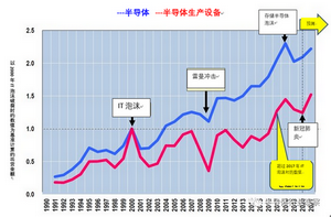
But there are also differences between the two.
Semiconductor shipments recovered soon after the IT bubble burst, and exceeded
the shipment value of the IT bubble in 2004. Later, after excluding the
"Lehman shock", the decline was basically an upward trend. In 2018,
the shipment amount reached 2.3 times that of the IT bubble.
On the other hand, as far as the shipment value of semiconductor production equipment is concerned, there has been a sharp decline after the IT bubble, but it has not recovered like semiconductors. Shipments in 2007 and 2011 were basically close to the IT bubble, but did not exceed the IT bubble. Three years ago, in 2017, it exceeded the IT bubble for the first time.
In other words, it took 17 years to exceed the peak in 2000! Why did it take so long? Also, why has the shipment value of semiconductor production equipment increased rapidly after entering 2017?
The Main Reason Preventing the Growth of Semiconductor Production Equipment Sales Volume
The author believes that there are two main reasons why it is difficult for the shipment value of semiconductor production equipment to exceed the peak of the IT bubble. One is the reduction of cutting-edge semiconductor manufacturers, and the other is the increase in throughput (Through Put, the number of wafers processed in one hour) of various production equipment. Detailed below.
First, the reduction of cutting-edge semiconductor manufacturers. For example, as far as DRAM is concerned, after 2000, Japanese companies continued to abandon DRAM production. In addition, in 2000, Taiwanese companies continued to abandon DRAM production. In addition, Qimonda, which was independent from Germany's Infineon Technologies in 2006, also closed down in 2009. The only remaining Japanese company, Elpida Storage Semiconductor, also closed down in 2012 and was acquired by Micron Technology of the United States. In the end, only Samsung, SK hynix, and Micron DRAM manufacturers remained.
In addition, as far as logic semiconductors are concerned, more and more manufacturers have given up research and development of cutting-edge miniaturization. For example, in August 2018, GLOBALFOUNDRIES of the United States announced that it would abandon research and development after 10 nanometers, so cutting-edge miniaturization technologies are concentrated in Intel and Samsung. , TSMC three companies. In addition, since 2016, Intel’s 10-nanometer startup has not been smooth, and the development of 7-nanometer and subsequent miniaturization is actually mainly concentrated in Samsung and TSMC.
As more and more semiconductor manufacturers are eliminated, fewer companies can make huge investment in equipment. Therefore, it is difficult for the shipment amount of semiconductor production equipment to increase.
Increase in throughput of various semiconductor production equipment (Through Put, the number of wafers processed in one hour)-"Doing a cocoon"
The second main reason is that various semiconductor production equipment manufacturers strive to increase the throughput of wafers (this reason is really ironic).
For example, when liquid immersion ArF exposure equipment appeared around 2007, the throughput was 130 units/hour, but today's throughput can exceed 250 units/hour. In other words, in 2007, two liquid immersion ArF exposure equipment were needed, but today only one is needed.
An even more incredible example is cleaning equipment. As we all know, semiconductor cleaning equipment has a "batch type" that processes 50 wafers at a time and a "monolithic type" that processes one by one. Of course, the throughput of the "batch type" is much greater than that of the "single chip", but the "batch type" has a disadvantage, that is, stains after cleaning are easy to remain on the wafer; although the "single chip" does not The shortcomings of residual stains, the throughput is not high.
However, as far as "single chip" equipment is concerned, the cleaning tanks that can be mounted on a device's platform (Platform) gradually increase to 4→8→16→24. Therefore, the throughput of "single chip" is not inferior. In the "batch type", it even reached 800 per hour. As a result, with 2008 as a watershed, the "protagonist halo" of cleaning equipment has shifted from "batch type" to "single chip type." As shown in Figure 3.
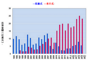
The only advantage of the “batch type” used to be
higher throughput. If the “monolithic type” that solves the problem of stain
residue can obtain the same amount of throughput, there is no reason to
continue to use the “batch type” equipment. In other words, since 2014, the
reason why the shipment value of "batch-type" equipment has increased
is because the production of 3D NAND flash memory (hereinafter referred to as
"NAND") requires the use of batch-type wafer etching equipment, and
The demand is constantly growing.
What makes people feel incredible is that although semiconductor manufacturers have greatly increased the throughput of their equipment through their own efforts, the prices of the equipment themselves have not increased proportionally, that is to say, the manufacturers of the equipment have "had a cocoon".
Then, why after 2017, the amount of shipments of semiconductor production equipment will exceed that of the IT bubble in 2000, and have seen rapid growth?
3D NAND
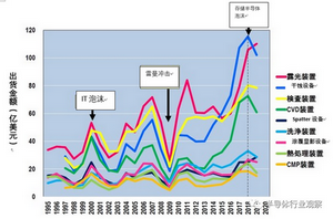
Figure 4 below is the transition table of the shipment amount of various production equipment. Before 2015, the shipment value of exposure equipment has been ranked first. After 2015, dry etching (Dry Etching) equipment began to rank first. In addition, the shipment value of CVD equipment has also grown rapidly. In 2017, the shipment value of CVD equipment was almost close to exposure equipment and inspection equipment.
The author believes that the main reasons are the
following: the big data era has officially arrived, the demand for data centers
has soared, and the demand for storage semiconductors in the direction of
servers has grown rapidly. Especially the 3Dization of NAND in storage
semiconductors has played an important role.
The storage density is increasing at a rate of 1.5 times every year. Therefore, the number of layers of 3D NAND is also increasing: 24 layers → 32 layers → 48 layers → 64 layers → 96 layers → 128 layers. For example, increasing from 64 layers to 96 layers requires 1.5 times the number of CVD equipment in theory.
In addition, the number of dry etching equipment required is not only increased by 1.5 times, that is, it takes about one hour to open the memory hole (Memory Hole) of a 64-layer 3D NAND. However, the deeper the opening, the slower the etching speed, so it takes many hours to open the 96-layer storage hole.
However, only Samsung Electronics is currently processing a 96-layer (92-layer to be precise) memory hole. The 96-layer of Kioxia and other companies uses a stack of two 48-layers. Since the 48-layer HARC etching is performed twice, twice as much dry etching equipment is required.
As a result, due to the 3D NAND and the increase in the number of layers, the demand for various devices is also increasing. The direct result is that the amount of shipments of semiconductor production equipment exceeded the peak of the IT bubble in 2017.
The storage semiconductor market reached its peak in 2018, and storage semiconductors fell into a trough in 2019. It is predicted that after 2020, storage semiconductors will grow again, and the amount of semiconductor production equipment shipments will also grow again.
Effect of EUV
As shown in Figure 4, due to the downturn in storage semiconductors in 2019, the shipment value of many semiconductor devices has fallen. However, the shipment amount of exposure equipment has been increasing. As a result, the shipment value of exposure equipment in 2019 once again ranked first in TOP1. This is mainly due to the official popularization of EUV, the most cutting-edge exposure equipment priced at 16 billion yen (about 960 million yuan) per set.
At the "VLSI Symposium" held in June 2020, ASML announced that it had shipped 53 EUV devices (3400 series) in the fourth quarter of 2019. As shown in Figure 5 below, the number of sales in the first quarter of 2020 has increased 4 units, therefore, a total of 57 EUV devices have been sold in the first quarter of 2020.
However, what is surprising is that on January 22, 2020, WikiChip Fuse reported that at the time of the fourth quarter of 2019, ASML’s EUV had 49 Open POs, and it was speculated that TSMC was 20. Samsung has 20 units, Intel has 4-5 units, and other Micron and SK hynix are small.
According to industry insiders familiar with Lithography, after 2020, TSMC will import more than 20 EUV equipment every year. In addition, it is said that Samsung Electronics also plans to introduce 20 EUV exposure equipment every year from 2020. Based on this calculation, the two companies will start more than 100 EUV exposure equipment in total in 2025. Affected by the effect of EUV, the shipment amount of exposure equipment will also increase substantially in the future.
In addition, as far as EUV peripheral equipment is concerned, the shipment value of mask drawing equipment, mask inspection equipment, and coating development equipment (Coater Developer) will also increase.
Market Share and Future Prospects of Various Semiconductor Production Equipment Manufacturers
Finally, let’s
take a look at the market share of various semiconductor production equipment
companies in 2019 (see Figure 6 below). South Korea’s SEMES and China’s NAURA
have also gained a certain market share in some areas, but in terms of overall
equipment In other words, it is basically divided up by Japanese, American, and
European companies.
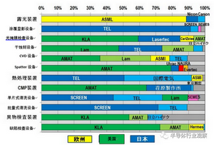
Exposure equipment, coating and developing equipment (Coater Developper), sputtering equipment (Spatter), batch-type cleaning equipment, foreign body inspection equipment, defect inspection equipment are almost in the "one super multi-strength" model, in addition, photomask inspection equipment, CVD equipment, heat treatment equipment, CMP equipment, and single-chip cleaning equipment are the "two super and more powerful" models. In addition, the dry erosion equipment is almost a "three super one strong" model.
In short, as far as all semiconductor production equipment is concerned, certain companies in Japan, Europe, and the United States have created a "1 super-3 super + other" model, that is to say, these companies have brought together the technical essentials of semiconductor production equipment, new It is difficult for companies to enter. Although China is pushing hard for the localization of semiconductor production equipment, the research and development of cutting-edge production equipment takes a long time.
So, what is the trend of the future shipment value of semiconductor production equipment? Judging from past experience, the amount of shipments of semiconductor production equipment is more obvious than the fluctuation of the semiconductor itself. In the future, there should be phenomena such as "some bubble" and "something shock". By then, the amount of shipments of semiconductor production equipment There will be substantial changes.
However, the miniaturization of logic semiconductors has not stopped. In addition, the miniaturization of DRAM will continue to progress, and at the same time, the number of layers of 3D NAND should continue to increase. Therefore, the author firmly believes that although the amount of shipments of semiconductor production equipment may fluctuate significantly, the overall trend is increasing, at least not affected by the COVID-19, and continue to grow.
*Disclaimer: The reprint of Semiconductor Industry Observation is only to convey a different point of view. It does not mean that Semiconductor Industry Observation agrees or supports this view. If you have any objections, please contact Semiconductor Industry Observation.